+
WEBINAR: Unlock the Power of Industrial CT Scanning
See Deeper. Solve Faster. Spend Smarter.
A 1/2 Hour That Could Reshape Your Inspection Strategy
Date: Wed June 18, 2025
Time: 11am Central Time
Location: Live Online Webinar
See Deeper. Solve Faster. Spend Smarter.
A 1/2 Hour That Could Reshape Your Inspection Strategy
Date: Wed June 18, 2025
Time: 11am Central Time
Location: Live Online Webinar
See Deeper. Solve Faster. Spend Smarter.
A 1/2 Hour That Could Reshape Your Inspection Strategy
Date: Wed June 18, 2025
Time: 11am Central Time
Location: Live Online Webinar
Analyze solder joints, PCB structures, internal defects, and electromechanical interactions with industrial CT scanning before teardown or destructive testing.
Electronic assemblies continue to advance. Are manufacturing inspection strategies keeping up?
Higher component density, finer-pitch geometries, stacked architectures, and multi-layer PCB designs have pushed electronics into areas where common inspection methods struggle to deliver clear data. Automotive electronics, aerospace systems, medical devices, battery technologies, and high-performance consumer products are pursuing long-term stability. A single hidden defect within a solder joint or an internal layer can undermine their abilities.
Identifying defect size, location, severity, and relationship to surrounding structures without damaging the workpiece becomes the challenge.
Industrial CT scanning as a validation and analysis tool has become increasingly valuable for electronics manufacturers focused on reliability.
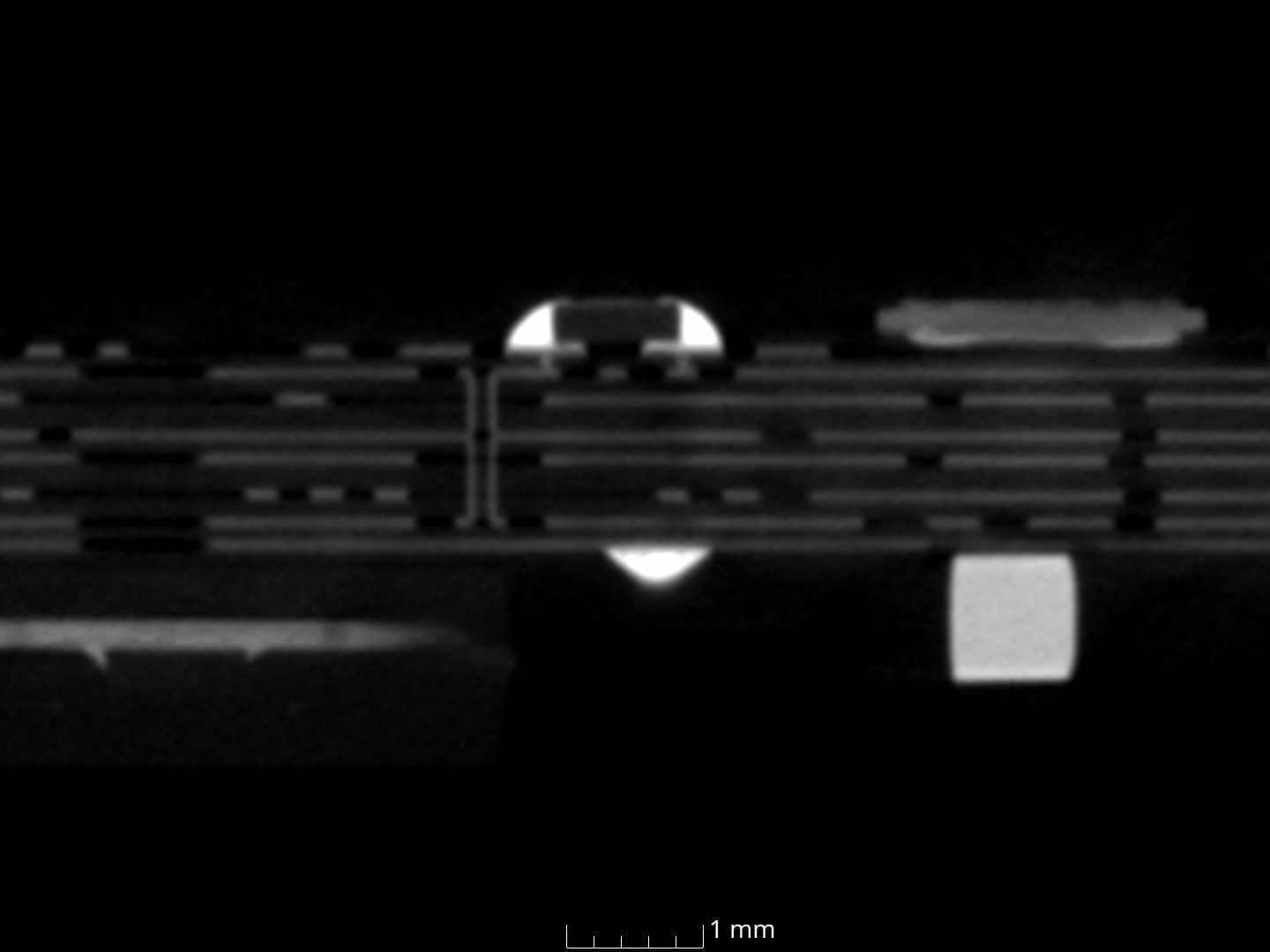
At Nel PreTech Corporation (NPC), industrial X-ray computed tomography is used to evaluate internal electronic structures in three dimensions. Engineering teams will see solder voids, delamination, poor interconnect formation, cracked joints, internal misalignment, and concealed assembly defects that are tough to see with conventional inspection techniques.
Most electronics failures quietly develop long before a device stops working.
A board may pass electrical testing while internal degradation is already developing beneath a BGA package. A solder joint may appear acceptable in a two-dimensional X-ray image, yet excessive voiding can reduce thermal transfer capability. Internal layer separation inside a PCB may remain undetected until thermal cycling or vibration causes intermittent failures in the field.
Modern assemblies are exposed to increasingly aggressive operating conditions, including:
As assemblies become smaller, acceptable process variation becomes smaller as well.
For quality engineers and manufacturing teams, this creates a difficult inspection problem: many reliability-critical defects exist entirely inside the product.
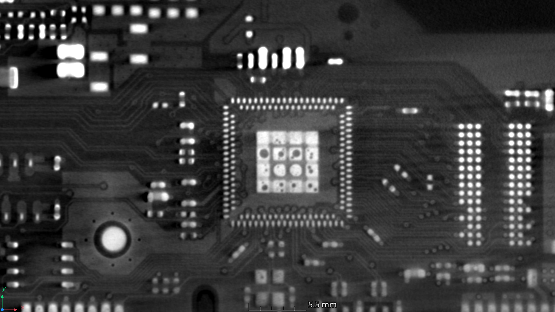
Industrial CT scanning is used to evaluate complete internal assembly geometry non-destructively. Instead of assessing overlapping grayscale projections, CT reconstruction generates a volumetric dataset that can be sliced, segmented, rotated, and analyzed layer by layer.
This level of inspection is ideal for evaluating complex solder structures and densely populated electronics.
Solder voiding remains one of the most common findings during electronics CT inspection.
Voids typically develop from trapped flux volatiles, contamination, outgassing, improper reflow conditions, or process inconsistencies during assembly. While some amount of voiding may fall within acceptable limits, other concentrations can affect thermal dissipation and mechanical integrity.
Industrial CT scanning capabilities:
This becomes especially meaningful in power electronics, battery systems, automotive control modules, and high-current applications where thermal management affects long-term performance.
Unlike conventional radiography, CT scanning isolates the solder joint in 3D. This makes it possible to evaluate individual connections without interference from overlapping structures.
Not all solder defects present as dramatic failures.
Some of the biggest reliability issues come from subtle process variation during assembly. Incomplete wetting, insufficient solder flow, weak surface bonding, and partially formed joints may function properly early on. But, at the same time, be vulnerable to premature fatigue failure.
These conditions are often difficult to identify during visual inspection, especially when joints are concealed beneath components.
CT scanning provides cross-sectional visibility into the actual solder geometry, allowing engineers to evaluate:
For failure analysis investigations, this additional dimensional insight can significantly improve root cause identification.
Multi-layer PCBs rely on stable bonding between conductive and substrate layers throughout the product lifecycle.
Thermal stress, material incompatibility, manufacturing inconsistencies, or environmental exposure can contribute to internal separation between layers. In some cases, delamination may begin on a small scale before spreading into larger structural defects.
Industrial CT scanning can look at:
Rather than physically sectioning the board, engineers can inspect the internal structure while preserving the assembly for continued analysis or validation testing.
As electronic packaging density increases, inspection complexity increases with it.
Miniaturized electronics often pack a lot into a small space. They have stacked structures and embedded components. Miniaturized electronics also have tightly integrated heat management systems. It is hard to figure out how well these systems work using basic electrical testing methods.
CT scanning is particularly effective for:
Full-volumetric reconstruction using CT enables engineers to digitally section the assembly in any orientation without physically altering the piece.
This capability is extremely useful during product development, process qualification, and failure investigations where protecting the component is critical.
Electronic failures are not always purely electrical.
In many products, especially medical devices, sensors, electromechanical assemblies, and other highly integrated systems, electrical performance is closely tied to mechanical integrity. A device may exhibit an electrical failure symptom while the root cause originates from a mechanical issue, or vice versa.
For example, a cracked housing may place stress on an internal circuit board. A damaged solder joint may create intermittent electrical connectivity during operation. Mechanical wear, deformation, component shifting, or material fatigue can alter the performance of electrical pathways over time.
When investigating failed products, engineers often need to evaluate both systems simultaneously.
Industrial CT scanning provides a complete three-dimensional snapshot of the assembly before any teardown or destructive analysis occurs. This allows engineering teams to examine the relationship between electrical and mechanical features in their original state, preserving evidence that may be altered or lost during disassembly.
CT inspection can reveal:
This capability is particularly valuable during failure investigations because it allows engineers to document the complete condition of the product before taking it apart.
Rather than focusing on electrical or mechanical systems independently, CT scanning provides a comprehensive view of how the entire assembly functions as an integrated system. Engineers can identify whether a failure originated from an electrical defect, a mechanical issue, or an interaction between the two, leading to more informed root cause analysis and corrective action decisions.
Conventional inspection methods continue to play an important role in electronics manufacturing, but each technique has practical limitations when evaluating complex internal geometries.
Visual inspection remains effective for verifying external conditions such as:
However, it cannot evaluate concealed interconnects or internal structural integrity.
Traditional X-ray systems provide valuable internal visibility, but the resulting image is still a compressed projection of three-dimensional geometry.
As assembly density increases, overlapping features can obscure critical defects or complicate interpretation.
This becomes especially challenging in:
CT scanning eliminates much of this ambiguity by reconstructing the full internal volume.
Cross-section analysis provides highly detailed internal information, but it permanently destroys the sample.
For expensive prototypes, limited production parts, or mission-critical hardware, destructive analysis may not be practical.
Industrial CT scanning allows many of the same internal conditions to be evaluated while maintaining part integrity.
One of the most valuable aspects of CT inspection is not simply defect detection. It is defect characterization.
A volumetric dataset allows engineers to move beyond “pass/fail” inspection and understand how internal conditions relate to manufacturing processes and long-term reliability behavior.
CT-based analysis can support:
Measurements can be performed directly within the reconstructed volume using specialized software. Precise localization and quantitative analysis become feasible.
Industrial CT scanning has become increasingly popular in industries where CT supplier accreditation and traceability requirements continue to tighten.
Automotive systems must handle long-term vibration, thermal cycling, and harsh environmental factors. CT scanning is commonly used to evaluate ECUs, power electronics, battery assemblies, and sensor packages.
Mission-critical aerospace and defense systems require extensive internal verification. This reduces reliability risk in high-consequence operating environments.
Medical electronics often combine miniaturization with extremely high quality expectations. CT inspection provides internal validation without damaging expensive or highly regulated assemblies.
Battery modules, battery management electronics, and power conversion systems frequently require detailed evaluation of internal interconnects, welds, and thermal pathways.
As consumer products continue to shrink while increasing functionality, manufacturers are relying more heavily on advanced non-destructive inspection to identify assembly variation early in production.
Many defects that cause reliability issues exist beneath the surface. They are within solder joints, between PCB layers, or within enclosed assemblies, where external inspection offers limited insight.
Industrial CT scanning brings 3D inspection capabilities to those internal structures non-destructively. It provides a much deeper understanding of assembly integrity and defect formation.
At Nel PreTech Corporation, industrial CT scanning is part of advanced inspection and failure analysis workflows. Our services support electronics manufacturers, quality engineers, and product development teams working with increasingly complex designs.
Whether the objective is solder void analysis, PCB inspection, hidden defect detection, reliability validation, or root cause investigation, CT scanning can provide the internal visibility needed to make more informed engineering decisions.
In addition to identifying solder defects and PCB-related issues, CT scanning helps engineers understand how electrical and mechanical systems interact, providing a complete picture of product condition before destructive analysis begins.
Reach out to our CT experts to discuss your next electronics project before you start teardown.

Antonio “AJ” Gradi is curious and eager to always learn new information. That dedication to knowledge has catapulted him from Applications Engineer/ CT Specialist to Director of CT at Nel Pretech Corporation. AJ joined the 3D scanning and industrial CT laboratory in July of 2022 and has excelled in every task given.

You'll find all the detailed service information you need in one brochure.
Download Brochure
Get a quote within 24-hours and keep your project on schedule.
Get a Quote
Our Nel PreTech engineers are ready to get started on your product challenges.
Ask an Engineer
Download the ultimate CT Scanning Buyer's Guide to improve understanding, time, and efficiency in your scanning needs. Over 50 Pages of useful data and case studies.
Download Now